
| DSP | 1 C2x |
| DSP MHz (Max) | 40 |
| CPU | 32-bit |
| Rating | Military |
| Operating temperature range (C) | -55 to 125 |
- Military Temperature Range
- -55°C to 125°C
- 100-ns or 80-ns Instruction Cycle Times
- 544 Words of Programmable On-Chip Data RAM
- 4K Words of On-Chip Program ROM
- 128K Words of Data/Program Space
- 16 Input and 16 Output Channels
- 16-Bit Parallel Interface
- Directly Accessible External Data Memory Space
- Global Data Memory Interface
- 16-Bit Instruction and Data Words
- 16 × 16-Bit Multiplier With a 32-Bit Product
- 32-Bit ALU and Accumulator
- Single-Cycle Multiply/Accumulate Instructions
- 0 to 16-Bit Scaling Shifter
- Bit Manipulation and Logical Instructions
- Instruction Set Support for Floating-Point Operations, Adaptive Filtering, and Extended-Precision Arithmetic
- Block Moves for Data/Program Management
- Repeat Instructions for Efficient Use of Program Space
- Eight Auxiliary Registers and Dedicated Arithmetic Unit for Indirect Addressing
- Serial Port for Direct Code Interface
- Synchronization Input for Synchronous Multiprocessor Configurations
- Wait States for Communication to Slow-Off-Chip Memories/Peripherals
- On-Chip Timer for Control Operations
- Three External Maskable User Interrupts
- Input Pin Polled by Software Branch Instruction
- 1.6-um CMOS Technology
- Programmable Output Pin for Signaling External Devices
- Single 5-V Supply
- On-Chip Clock Generator
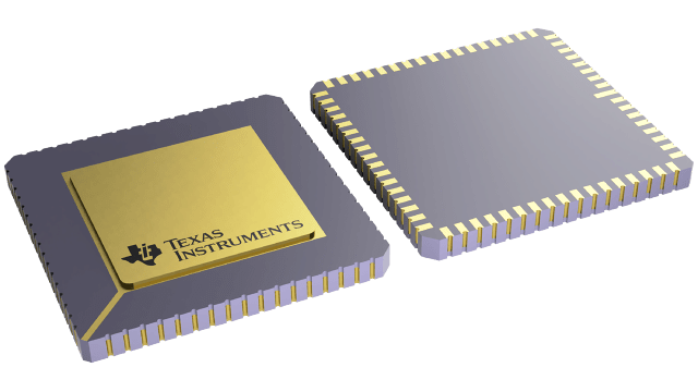
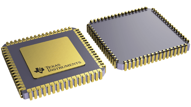
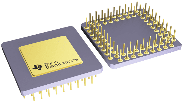
- Packaging:
- 68-Pin Leaded Ceramic Chip Carrier (FJ Suffix)
- 68-Pin Ceramic Grid Array (GB Suffix)
- 68-Pin Leadless Ceramic Chip Carrier (FD Suffix)
SMJ320 is a trademark of Texas Instruments Incorporated.
This data sheet provides design documentation for the SMJ320C25 and the SMJ320C25-50 digital signal processor (DSP) devices in the SMJ320? family of VLSI digital signal processors and peripherals. The SMJ320 family supports a wide range of digital signal processing applications such as tactical communications, guidance, military modems, speech processing, spectrum analysis, audio processing, digital filtering, high-speed control, graphics, and other computation-intensive applications.
Differences between the SMJ320C25 and the SMJ320C25-50 are specifically identified, as in the following paragraph and in the parameter tables on pages 18 through 24 of this data sheet. When not specifically differentiated, the term SMJ320C25 is used to describe both devices.
The SMJ320C25 has a 100-ns instruction cycle time. The SMJ320C25-50 has an 80-ns instruction cycle time. With these fast instruction cycle times and their innovative memory configurations, these devices perform operations necessary for many real-time digital signal processing algorithms. Since most instructions require only one cycle, the SMJ320C25 is capable of executing 12.5 million instructions per second. On-chip data RAM of 544 16-bit words, on-chip program ROM of 4K words, direct addressing of up to 64K words of external data memory space and 64K words of external program memory space, and multiprocessor interface features for sharing global memory minimize unnecessary data transfers to take full advantage of the capabilities of the instruction set.


